Designing Fixtures in PCB Rigid Flex
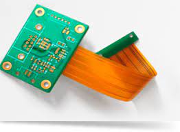
Rigid flex circuit boards allow the design of electronic devices that are flexible enough to fold, roll and twist into various shapes. By eliminating external wiring harnesses and connectors, these circuit boards can reduce assembly time and improve product design flexibility. Additionally, they are able to withstand repeated bending cycles that would break solder joints on rigid PCBs, making them an excellent choice for mechanisms that need rugged, portable, lightweight circuitry.
PCB rigid flex has become an industry standard for consumer and wearable electronics, as well as automotive and aerospace applications that require durable, light-weight, space-efficient components. They are also ideal for mobile phone and tablet manufacturers seeking to create compact, portable products that are easy to hold and operate. Rigid flex PCBs are lighter than traditional circuit boards, as they eliminate the need for backplanes and ribbon cables, which contribute to product weight and complexity. They are also more resilient than traditional PCBs, as their flex areas are capable of absorbing vibrational stresses that might fracture solder joints and other rigid board connections.
While the flexibility of rigid flex circuits offers numerous benefits, they are not without their challenges. During the design process, engineers must consider a variety of factors to ensure that their flexible circuits can withstand the stresses and environmental conditions that they will encounter in the field. This includes optimizing the rigid-flex stackup configuration, addressing mechanical durability concerns, and conducting thorough electrical testing.
The stackup configuration of a pcb rigid flex is critical to ensuring that the conductive layers and flex areas are adequately interconnected. Careful attention to layer arrangement facilitates streamlined routing and minimizes impedance distortion across the circuit board. Incorporating thermal vias into the rigid-flex stackup also allows for heat dissipation, improving temperature management and enhancing functional reliability.
Key Considerations for Designing Fixtures in PCB Rigid Flex
Another crucial aspect of rigid flex PCB design involves verifying that the bend radius compliance of the flexible areas meets specifications. Specified bend radii are designed to prevent mechanical stress on conductive traces, which can impact signal integrity and overall performance. Using tools that offer real-time connectivity to the flexible conductive area can help designers and engineers identify issues with the bend radius before they go to production, avoiding needless expenses.
The use of stiffeners in a flex PCB is necessary to provide adequate structural support that preserves the board’s inherent flexibility. However, stiffeners must be carefully selected and placed to avoid imposing unnecessary stress on the flex sections and rigid section of the circuit board. Considering these factors helps engineers optimize a flexible PCB’s stiffness and strength to meet operational requirements while maintaining flexibility.
For best results, it’s important to keep the number of layers on a rigid-flex PCB to a minimum. A high number of layers increases the cost and difficulty of manufacturing, as it requires more materials, additional labor, and extensive lamination processes. A reduction in the number of layers also reduces assembly time and costs, as there are fewer parts to solder and connect. Furthermore, limiting the number of layers allows for greater panel utilization and can minimize waste from selective plating or dual surface finish operations.